
A Tiny Stretch Gives Magic-Angle Graphene a Powerful New Control Knob
Published November 13, 2026
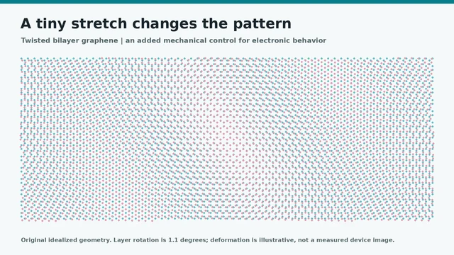
Original idealized lattice illustration; deformation is explanatory, not a measured sample image.
Researchers deliberately strained twisted graphene and measured an unusually strong resistance response. It is a new physics experiment, not a faster computer.
The wrinkle researchers usually try to eliminate has become a control knob.
In experiments on two extraordinarily thin sheets of carbon, a University of Washington team deliberately stretched and compressed the material. Small changes in strain produced unusually large changes in electrical resistance. The response was more than 100 times stronger than in an ordinary metal, according to the university's November 12 account of the study.
That is not a report of a computer running 100 times faster. It is a new way to manipulate a material whose electrical behavior is exceptionally sensitive to its geometry. For researchers trying to understand superconductivity and neighboring electronic states, that distinction is where the interesting physics begins.
Two Sheets and a Very Small Twist
Graphene is a sheet of carbon one atom thick. Stack two sheets and rotate one slightly relative to the other, and their repeating atomic arrangements produce a larger interference pattern called a moire pattern.
The effect has an everyday visual cousin: overlap two fine meshes and turn one. Large bands and shapes appear even though neither original mesh contains those shapes by itself. In graphene, however, the pattern does more than change what an observer sees. It changes the environment in which electrons move.
Earlier work found that near a twist angle of 1.1 degrees, and at temperatures close to absolute zero, the two-layer system can become superconducting. Researchers subsequently used temperature, magnetic field and electrical controls to investigate different states. The attraction is not simply obtaining one remarkable material. It is being able to explore several related states within a closely controlled system.
Manufacturing that system is difficult. The layers are microscopic, and laying one onto the other without stretching or distorting it is a delicate operation. An unintended deformation can change the pattern and complicate comparisons between devices.
The Washington researchers asked what would happen if they controlled that deformation instead of treating it only as an unwanted error.
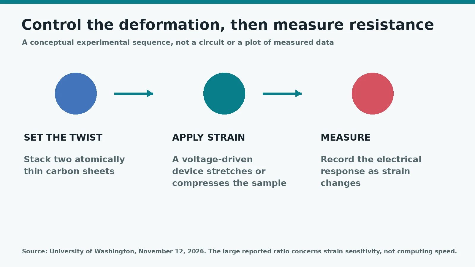
Original experimental overview, not a wiring diagram or fabricated resistance plot.
Turning a Defect Into an Experiment
The team attached the tiny material flakes to a device that expands or contracts when voltage is applied. That provided a way to adjust strain continuously rather than comparing separate samples that happened to contain different distortions.
As the lattice was deformed, electrical resistance changed dramatically. Cooling the sample to very low temperatures amplified the response further. The work, published November 12 in Science, adds mechanical deformation to the variables scientists can deliberately change while studying the electronic system.
The important comparison concerns sensitivity: how strongly the resistance responds to strain relative to an ordinary metal. It does not mean resistance simply fell a hundredfold, that all conditions produced superconductivity, or that a finished device offers a hundredfold improvement in efficiency.
This is why the experiment is more interesting than a large number in isolation. If a small mechanical change strongly reorganizes electrical behavior, it gives researchers another route into the relationship between the material's geometry and its collective electron behavior.
A Research Tool Before a Product
There is a long distance between a delicate, very cold laboratory sample and an inexpensive component in an everyday machine. The team wants to simplify the experimental arrangement so other researchers can reproduce it more easily and apply the approach to other atomically thin materials.
That next step is practical in a scientific sense: make the control more accessible, compare results and find out which effects are general. It is not yet a manufacturing roadmap for a new processor or a room-temperature power grid.
The broader question is why striking responses to strain appear in other unusual electronic materials too, including high-temperature superconductors. A controllable model system can help researchers investigate connections that would be difficult to separate in a less adjustable material.
For makers, the appealing idea is familiar even if the equipment is not. A variable that initially looks like a source of bad tolerances can become useful once it is measurable and controllable. Here that variable is deformation on an atomic scale, and the output is a surprisingly large electrical response.
Which is the more exciting prospect: a useful strain-sensitive device, or a better experiment for understanding superconductivity? Join the comments below.
Comments
Member comments are temporarily unavailable.
Log in to join the discussion.